
A 12 V supply has to power a 5 V electronic board drawing 2 A. A linear regulator could discard the extra voltage as heat: (12 − 5) × 2 = 14 W. A switching buck converter can be much more efficient, yet its inductor current deliberately rises and falls thousands of times each second. Why tolerate that ripple?
The ripple is the mechanism that transfers energy. A switch alternates the voltage across an inductor; the inductor converts each voltage pulse into a controlled change of current. A capacitor then absorbs the alternating part so that the load sees nearly steady voltage. The useful design question is how much current ripple to allow.
Two switch positions, one continuous current
Consider an ideal synchronous buck converter. A high-side MOSFET connects a switching node to the 12 V input; a low-side MOSFET connects it to ground during the complementary interval. An inductor runs from that node to the 5 V output. The output capacitor and load connect from the output to ground. The two MOSFETs must never be commanded on simultaneously.
When the upper switch conducts, the inductor sees approximately Vin − Vout = 7 V. Its current rises according to VL = L di/dt. When the lower switch conducts, the switching node approaches ground and the inductor sees −5 V, so its current falls. The inductor keeps current flowing through the load during both intervals. A diode can replace the lower MOSFET, with additional conduction loss.
At steady state, the inductor cannot accumulate current indefinitely. The average voltage across it over a complete cycle must be zero:
(Vin − Vout) D T + (−Vout)(1 − D) T = 0.
Here D is the fraction of the period with the upper switch on, and T = 1/fs is the switching period. Rearranging gives D = Vout/Vin, or 5/12 ≈ 0.417 in our ideal example. This is volt-second balance: the positive and negative areas under the inductor-voltage trace cancel. Real converters adjust duty cycle to accommodate resistance, switching drops and disturbances.
Putting a number on the ripple
Suppose the switching frequency is 250 kHz and the inductance is 10 µH. The period is 4 µs; the upper switch conducts for approximately 1.67 µs. During that interval the current rises by
ΔI = (Vin − Vout) D / (L fs) = (7 V × 0.4167)/(10 µH × 250 kHz) ≈ 1.17 A peak-to-peak.
The current falls by the same amount during the remaining 2.33 µs. For a 2 A load in continuous-conduction mode, its ideal triangular waveform therefore ranges from approximately 1.42 A to 2.58 A. These values are a calculated illustration, not measurements of a commercial regulator. The units work: volts times seconds divided by henries gives amperes.
Notice what the calculation predicts. Doubling L to 20 µH halves the ripple to about 0.58 A, but does not change the ideal 5/12 duty ratio. Raising the switching frequency also reduces ripple, although faster switching tends to increase transistor switching and gate-drive losses. Analog Devices’ AN-140 design note describes precisely these component-size, ripple and loss trade-offs.
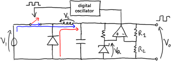

What the output capacitor actually does
The capacitor carries the difference between inductor current and load current. During the upper half of the triangular ripple it charges; during the lower half it discharges. With an ideal capacitor and constant load, the peak-to-peak voltage ripple is approximately ΔVout = ΔI/(8 fs C). For 47 µF, our 1.17 A ripple gives roughly 12.4 mV peak-to-peak. A real capacitor’s equivalent series resistance (ESR) adds an approximately ΔI × ESR component with a different waveform; 20 mΩ corresponds to about 23 mV of resistive swing. The contributions should not simply be assumed to peak at the same instant.
That calculation omits capacitor tolerance, DC-bias derating of ceramic capacitors, parasitic inductance and fast switching spikes. The LT1074/LT1076 design manual explains why capacitor ESR, layout and load transients matter alongside nominal capacitance.
Ripple also sets current stress. The approximate inductor RMS current for a triangular waveform is sqrt(Iout² + ΔI²/12), about 2.03 A here, while the 2.58 A peak must remain below the inductor’s saturation limit with appropriate margin. Analog Devices’ ADP5140 datasheet gives the same RMS and peak-current relationships and explicitly calls for checking saturation and thermal ratings.
The boundary where the simple equations stop working
At lighter load, the average current may become smaller than half the ripple. In a diode-based buck converter, current cannot continue below zero through the diode, so it reaches zero before the next switching cycle. This is discontinuous-conduction mode: the simple relation D = Vout/Vin no longer holds at fixed duty cycle. A synchronous converter can instead allow negative inductor current unless its controller prevents it. Controllers may also skip pulses to save energy at light load, changing ripple frequency and shape.
There is a second trap at start-up. The output is initially near zero, so the inductor sees almost the full input voltage during an on-pulse. A design sized only for nominal 5 V operation can experience different current slopes and stress while the output rises. AN-2582 documents how ripple can become substantially larger during soft start in high-duty-cycle designs. Short circuits, transient loads and current-limit behaviour deserve separate checks.
The comparison with a linear regulator is useful but incomplete: a buck converter adds switching noise, electromagnetic interference, control-loop stability concerns, inductor losses and layout sensitivity. The earlier Alkemata discussion of solar inverters and grid behaviour addresses a different scale of power conversion, where control and the surrounding system also determine what the hardware can actually deliver.
A practical design decision
For this 12-to-5 V example, a 10 µH inductor produces roughly 58% peak-to-peak ripple relative to the 2 A load. A 20 µH choice reduces it to 29%. Neither is universally better: the larger component may cost more, occupy more board area and have higher winding resistance, while the smaller one increases peak current, capacitor stress and potentially EMI. Compare candidate parts at their actual temperature, saturation rating, DC resistance and operating frequency before choosing.
One useful design habit follows from volt-second balance: begin with the two actual inductor voltages, calculate their durations and slopes, and only then choose the component. The current ripple is the trace of those switching decisions, and its size tells you what the rest of the circuit must survive.
Author
What concrete example would confirm or challenge this article?
Choose a reaction, write a comment, or ask your AI assistant to send a proposal for review. Comments are reviewed before publication.